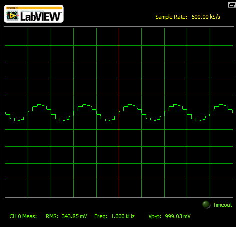
I just finished up an Operating Systems assignment and do not feel like getting too deep into software, so why not change things up and do a little hardware design! A sample and hold is used on the front end of an Analog to Digital Converter (ADC), and when it gets an impulse it will sample the input value and hold it until it resamples. This then allows the ADC to process the held value. In its simplest form a sample and hold can be implemented by a switch which causes the input to charge a small capacitor which is then buffered. If we were to construct this circuit we will get what is known as a staircase waveform. The following is a 1KHz sine wave, sampled at 10KHz.
Since we are sampling, we need to follow the Nyquist Rate or bad things (aliasing) will happen. To prove this, here we are just above the Nyquist Rate.
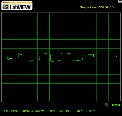
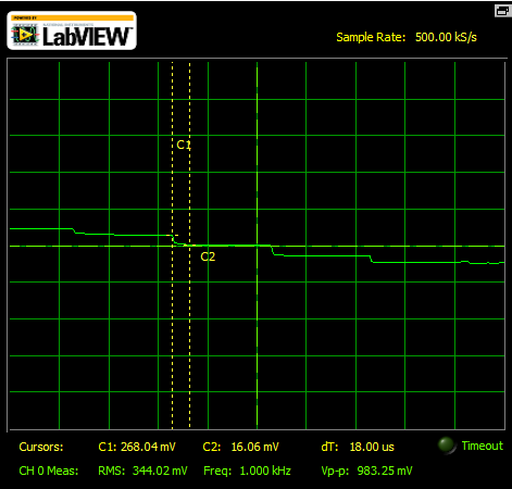
We ultimately want to assess the quality of the design so we need to look at droop rate and acquisition times.
An acquisition time of 16 microseconds isn't so bad! Now for the droop rate.
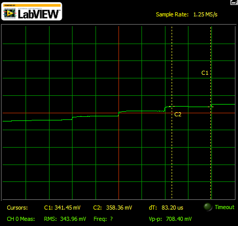
Which looks like 15.62 mV/ 86μs or 181.62 V/s. Droop rates and acquisition times are related. If we want to reduce the droop rate, we need a larger capacitor (or a buffer with a smaller input bias current), but that then will increase the acquisition time. The opposite is also true.
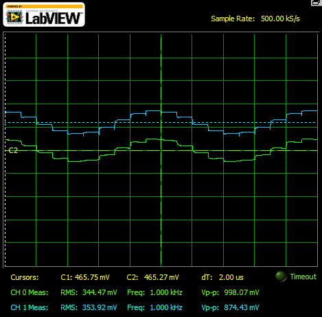
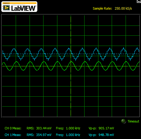
That's great but how does the design compare to an IC S&H? I hooked up a LF398 and got the following result.
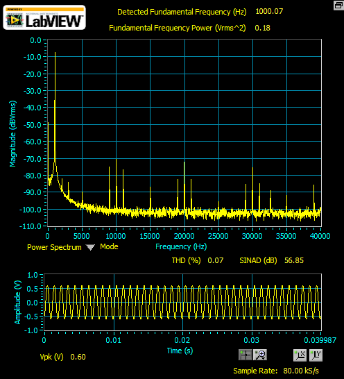
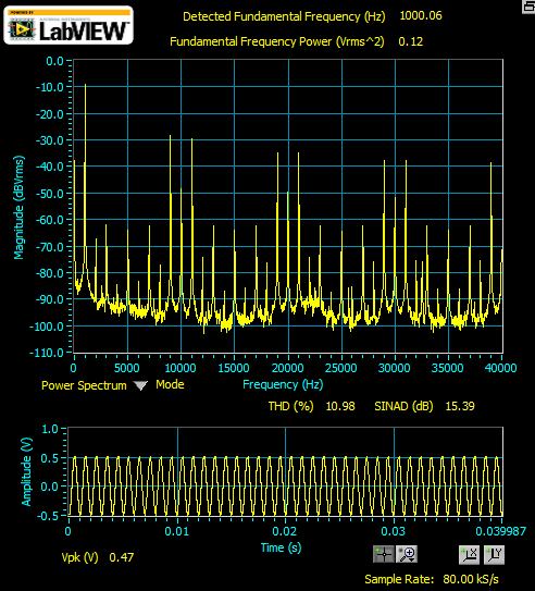
As for the harmonics, first we looked at the LF398, then our design.
Going back to the reconstructive filtering post, we can design a 3rd order filter to reconstruct back from the staircase signal.
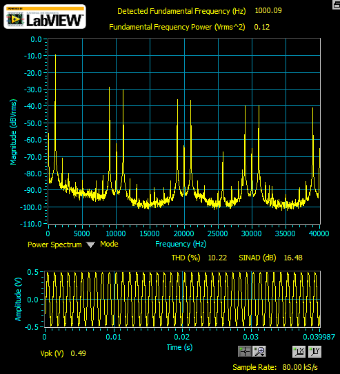
And as for the harmonics: